Optimizing for best photoresist adhesion
Tags:Update 2014-06-11: superseded.
- Objective:
- find the process which results in sharpest imprint after developing negative photoresist.
- Result:
- a reproducible process producing near-perfect imprints with resolution of 50 µm was found (marked as “final” in note body).
- Tools
- Materials
- Process (final)
- Process (used initially)
- Try #1
- Try #2
- Try #3
- Try #4
- Try #5
- Try #6
- Try #7
- Try #8
- Interlude: water break test
- Try #9
Tools
- Laminator
- ROYAL PL-2100, 120°C roller temperature
- Printer
- Brother DCP-7010R, Brother cartridge/toner
- UV Light
- 395nm 3W LED flashlight
- Exposure press
- 3.175mm clear acrylic sheet
Materials
- PCB
- 1.5mm epoxy/.035mm copper one-sided
- Photoresist
- negative dry film photoresist
- PCB cleaning fluid
- isopropanol 99.7% waterless
- Photoresist removal solution
- NaOH 5%wt
- Developer solution (final)
- K₂CO₃ 2%wt
- Developer solution (used initially)
- K₂CO₃ 5%wt
Process (final)
All operations with PCB are performed with latex gloves to avoid leaving fingerprints on it.
- Clean the PCB with isopropanol.
- Immerse PCB in NaOH for 10 min.
- Rinse PCB under warm tap water and wipe dry with soft lint-free cloth thoroughly.
- Remove matte (polyolefin) protective film from photoresist.
- Attach photoresist to PCB and put pressure on its front edge (any single edge) with fingers.
- Run PCB through laminator five times and let it cool down.
- Expose photoresist for 180 seconds (time calibrated for a particular setup).
- Remove glossy (PET) protective film from photoresist.
- Immerse PCB in developer solution for 1-2 minutes. Immediately after immersing, gently scrub with a soft acrylic brush until all unexposed areas are free from photoresist.
- Rinse PCB under warm tap water.
Process (used initially)
All operations with PCB are performed with latex gloves to avoid leaving fingerprints on it.
- Clean the PCB with isopropanol. After cleaning, expose to air until no traces of isopropanol are left.
- Remove matte (polyolefin) protective film from photoresist.
- Brush the PCB to remove any dust possibly present.
- Attach photoresist to PCB and put pressure on it with fingers.
- Run PCB through laminator and let it cool down.
- Expose photoresist for 180 seconds (time calibrated for a particular setup).
- Remove glossy (PET) protective film from photoresist.
- Develop the photoresist until all unexposed areas become wet and detach.
- Rinse PCB under warm tap water.
Try #1
Ambient temperature: 26°C.
This try was intentionally made with minimal precautions, to establish a quality baseline and determine which of the preparation steps are actually essential.
PCB was run through laminator once.
Photoresist was developed for 4 min.


Photoresist adhesion was poor. I’ve accidentally brushed against a corner before exposing and photoresist has detached from copper together with top protective film.
Quality: very low; very rough edges.
Photoresist was removed and board was reused for next try.
Try #2
Ambient temperature: 24°C.
PCB was run through laminator five times.
Photoresist was developed for 4 min.


Quality: better, varying. Edges are nicer, but thinnest line was not present. NaOH application from try #1 might have had an effect.

Photoresist was removed and board was reused for next try.
Try #3
Ambient temperature: 26°C.
This try intentionally follows try #1 to determine whether cleaning with NaOH had any positive effect.
PCB was run through laminator once.
Photoresist was developed for 4 min.


Quality: better edges than try #1, worse adhesion than try #2.
Photoresist was removed and board was reused for next try.
Try #4
Ambient temperature: 26°C.
PCB was run through laminator five times.
Photoresist was developed for 4 min.
After developing, PCB was gently scrubbed with a soft acrylic brush under warm tap water.


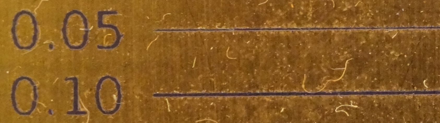
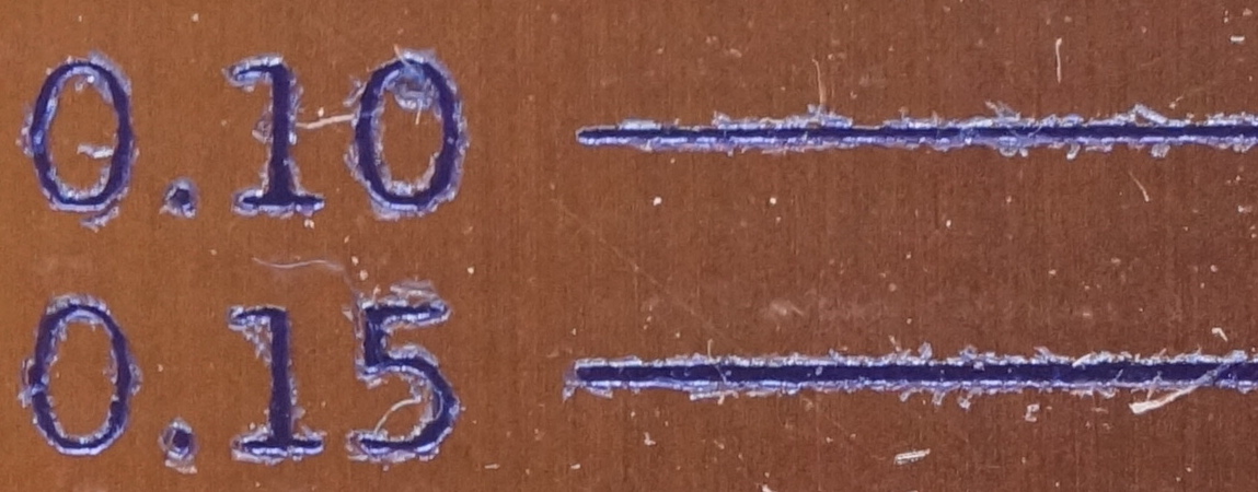
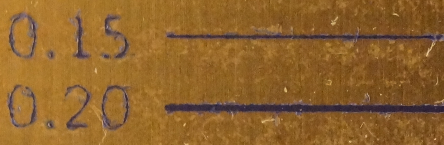
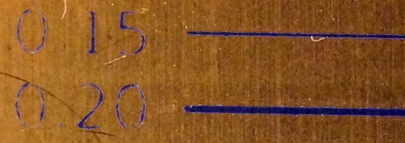
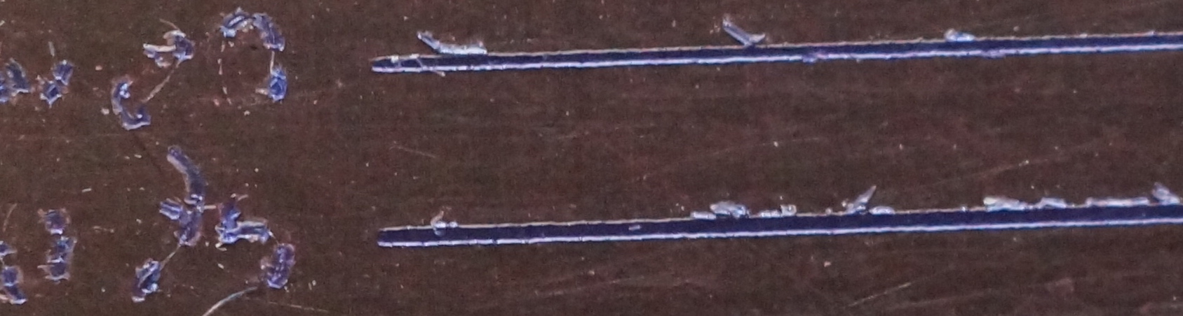
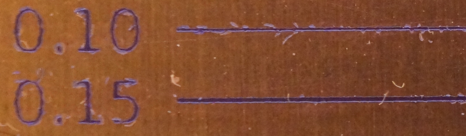
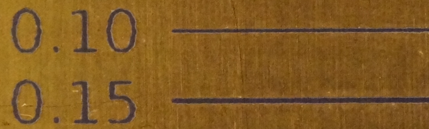
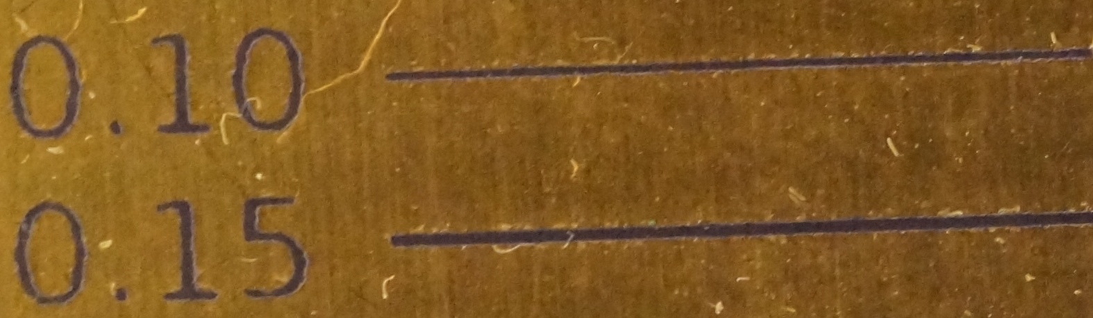
Quality: moderate. Visible gaps can be attributed to dust between photoresist and PCB. Smallest features are missing, but in uniform way; 0.15mm (6 mil) line is reliably reproduced.
Photoresist was removed and board was reused for next try.
Try #5
Ambient temperature: 26°C.
PCB was run through laminator five times. Photoresist was not entirely attached to PCB before lamination; only the front edge was pressed upon PCB.
I’ve forgot to measure the time photoresist was developed for, but it was likely more than 4 minutes.
While developing, PCB was gently scrubbed with a soft acrylic brush after resist started to visibly weaken / detach from board.


Quality: poor. It appears I have overdeveloped the resist. However, while I was brushing it in the solution, even smallest elements were clearly visible, much better than when I scrubbed it under tap water. It is likely that agitating the board reduces the time and solution concentration needed for developing.
Ideas to try:
- Begin to scrub the board immediately and not when resist starts to visibly detach.
- Reduce concentration of developer solution.
Photoresist was removed and board was reused for next try.
Try #6
Ambient temperature: 26°C.
This try verifies idea #1 from try #5.
PCB was run through laminator five times. Photoresist was not entirely attached to PCB before lamination; only the front edge was pressed upon PCB.
While developing, PCB was gently scrubbed with a soft acrylic brush immediately after immersion.


Quality: very good. For the first time, 0.1 mm line is not damaged. However, it is likely true that developer needs to have lower concentration.
Photoresist was removed and board was reused for next try.
Try #7
Ambient temperature: 26°C.
This try verifies idea #2 from try #5.
After cleaning, PCB was thoroughly wiped with lint-free cloth.
PCB was run through laminator five times. Photoresist was not entirely attached to PCB before lamination; only the front edge was pressed upon PCB.
New developer solution was used with concentration 2%wt.
While developing for 1 min, PCB was gently scrubbed with a soft acrylic brush immediately after immersion.


Quality: best so far. It appears that being thoroughly wiped of all residues of isopropanol is one of key requirements for good photoresist adhesion. Additionally, 2% developer solution didn’t work slower (or worse) than 5% one—if something, it was faster—an unexpected result. The board is a bit underdeveloped, however.
Photoresist was removed and board was reused for next try.
Try #8
Ambient temperature: 26°C.
After cleaning, PCB was thoroughly wiped with lint-free cloth.
PCB was run through laminator five times. Photoresist was not entirely attached to PCB before lamination; only the front edge was pressed upon PCB.
Developer solution used had concentration 2%wt.
While developing for 2 min, PCB was gently scrubbed with a soft acrylic brush immediately after immersion.


Quality: nearly perfect.
Interlude: water break test
Update 2014-02-24: see On water break test.
I’ve noticed that the very first try, despite horribly selected conditions, yielded one of the best imprints. I’ve also noticed that each time I clean the PCB from exposed (and unexposed) resist, there remains a visible ghost picture of the traces from previous try. Most of PCB (unexposed areas) is also clearly hydrophobic—meaning unexposed resist is not cleaned well enough.
I’ve decided to figure out the best way to clean board, using water break test to verify its condition. (Water break test in a nutshell: really clean copper is hydrophilic, contaminants are hydrophobic. Place PCB under water. If it’s really clean, a smooth, unbroken layer of water will remain.)
Test #1
PCB is immersed in NaOH for 2-4 min to remove old exposed resist, then scrubbed with isopropanol several times. (The procedure I’ve used earlier.)
Result: entire PCB is clearly hydrophobic. (Huh?!)
Test #2
PCB is immersed in NaOH for 2-4 min to remove old exposed resist, then scrubbed with isopropanol several times, then immersed in NaOH for 10 min again.
Result: entire PCB seems to be hydrophilic. I don’t have a standard to compare with, so I’m assuming this is “good enough”.
Try #9
Ambient temperature: 26°C.
PCB was cleaned with isopropanol, then immersed in NaOH for 10 min. Afterwards, PCB was rinsed in tap water and thorougly wiped with lint-free cloth.
PCB was run through laminator five times. Photoresist was not entirely attached to PCB before lamination; only the front edge was pressed upon PCB.
Developer solution used had concentration 2%wt.
While developing for 2 min, PCB was gently scrubbed with a soft acrylic brush immediately after immersion.


Quality: perfect. No defects due to poor photoresist adhesion are present; all visible defects are also present on photonegative. All features down to 50 µm are reproduced. (Photoresist resolution is about 40 µm.)