Producing PCBs using photolithography
Tags:In this note I describe a simple and quick photolithographic process with excellent repeatability that I use for producing high-quality PCB prototypes.
- Tools
- Materials
- Milling and drilling
- Photonegatives
- Preparation
- Exposure and development
- Etching
- Adding solder mask
- Tinning
Tools
- CNC machine
- CNC3020T
- laminator
- ROYAL PL-2100, 120°C roller temperature
- printer
- Brother DCP-7010R, Brother cartridge/toner
- magnetic stirrer
- MM-5M
- UV light source
- 395nm 3W LED flashlight
- latex gloves
- diamond-grip powder-free latex gloves
- exposure press
- d=3.175mm clear acrylic sheet
- soft brush
- generic soft acrylic brush
Magnetic stirrers may be expensive; I recommend building an open hardware one by Tekla Labs.
Materials
- toner density enhancer
- Density Toner by Kruse
- copper-clad laminate PCB
- any
- negative dry film photoresist
- generic
- negative dry film solder mask
- Dynamask 5000
- PCB cleaning fluid
- isopropanol 99.7% waterless
- preparation etchant
- (NH₄)₂S₂O₈ 15%wt
- developer solution
- K₂CO₃ 2%wt
- trace etchant
- FeCl₃ 50%wt
- resist removal solution
- NaOH 5%wt
- tinning solution
- “liquid tin” (locally sourced); composition & preparation
Milling and drilling
I use pcb-gcode (settings) for EAGLE to produce G-code for drilling and milling. I draw a contour on the “Milling” layer to cut out the PCB.
Note that if your tools have different lengths, you should set the Z offset in the LinuxCNC tool table; the configuration includes the G43 code after tool changing sequence.
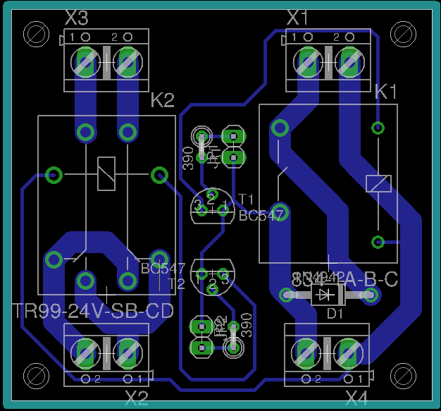


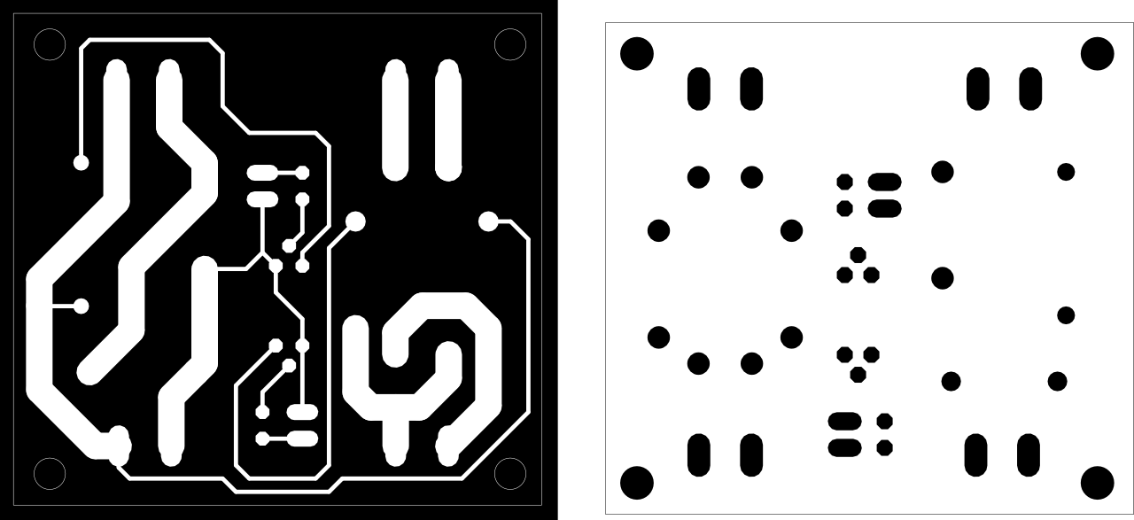
Photonegatives
I use Eagle’s CAM processor (configuration) to output photonegatives (copper and solder mask) as PostScript, process them with the ps2svg script, and then use Inkscape to combine them on a single A4 page. It is very important to not import PostScript directly to Inkscape; it is unable to import PostScript without spurious, hard-to-notice scaling.
After printing, I apply the “Density Toner” aerosol to the photonegatives to make the distribution of toner more uniform.


Preparation
Every step of handling PCB must be performed in gloves to avoid leaving grease. Grease on PCB surface generally results in a complete failure.
Earlier, I used a dilute NaOH solution for cleaning the copper surface and achieving better photoresist adhesion (note 1, note 2). However, it was a mistake. It turns out that a much better method exists:
- Clean the PCB surface from grease with isopropanol.
- Put the PCB into the persulphate etchant for 5-10 seconds. Note that other etchants may not have the same effect.
- Rinse PCB under warm tap water.
- Remove matte (polyolefin) protective film from photoresist.
- Attach photoresist to PCB and put pressure on its front edge (any single edge) with fingers.
- Run PCB through laminator and let it cool down.
This method results in excellent attachment (and a truly beautiful color). No matter how hard I scrub the PCB while developing, even the smallest traces of photoresist do not detach.
As far as I’m aware, the reason is that (specifically) persulphate etchant leaves the surface microporous, similar to the aluminium anodizing process.


Exposure and development
The exposure time may be affected by a lot of factors. It is best to determine optimal exposure time using a calibration pattern.
- Expose photoresist for calibrated time.
- Remove glossy (PET) protective film from photoresist.
- Immerse PCB in developer solution for 1-2 minutes. Immediately after immersing, scrub with a soft acrylic brush until all unexposed areas are free from photoresist.
- Rinse PCB under warm tap water.


Etching
I have found that persulphate-based etchant is very slow and tends to undercut traces. As such, I only use it for preparation, and etch the traces using ferric chloride.
It is very important for the etching liquid to be stirred. This significantly reduces etching time and, as a side effect, reduces trace undercutting.


Adding solder mask
Solder mask is very convenient to have on the PCB surface and isn’t complex to add once you already have a working photolithography process. The process for adding solder mask, as well as exposure time, are also very similar to the ones for photoresist:
- Remove matte (polyolefin) protective film from solder mask.
- Attach solder mask to PCB and put pressure on its front edge (any single edge) with fingers.
- Run PCB through laminator (if the solder mask is old and adheres poorly, do it 4-5 times) and let it cool down.
- Expose solder mask for calibrated time.
- Remove glossy (PET) protective film from solder mask.
- Immerse PCB in developer solution for 1-2 minutes. Immediately after immersing, scrub with a soft acrylic brush until all unexposed areas are free from solder mask.
- Cure solder mask; that is, expose it for ~10-30x longer than the first time.


Tinning
Chemical tinning is an excellent last step in the fabrication process that would make soldering much easier (even more so for SMD components). To perform it, simply put the board into the tinning solution for the time specified in the manual. In my case, it’s 15-30 min for 1µm thick tin layer.
