50W LC resonant converter, power board V1
Tags:In this note I will describe a part of a 50W resonant LC converter that I am designing. The converter will be modular: it will feature a control board with an Ethernet interface, a frontend board with a rectifier/multiplier and a matching network to allow current/voltage readouts, and a power board with the high-voltage transformer, its driver and signal isolation.
This note describes the first revision of the power board.
Objective
The immediate goal of the converter is to supply high-voltage, regulated DC for a magnetron sputtering chamber. A more general goal is to learn how to perform instrumentation and process control.
Design
The converter is a typical LC resonant converter. This topology is described in e.g. a Texas Instruments whitepaper Resonant Mode Converter Topologies by Bob Mammano. The key factor in selecting an LC resonant converter was the ease of regulating the output power by adjusting the frequency.
The circuit is as follows (see full design files on Github):
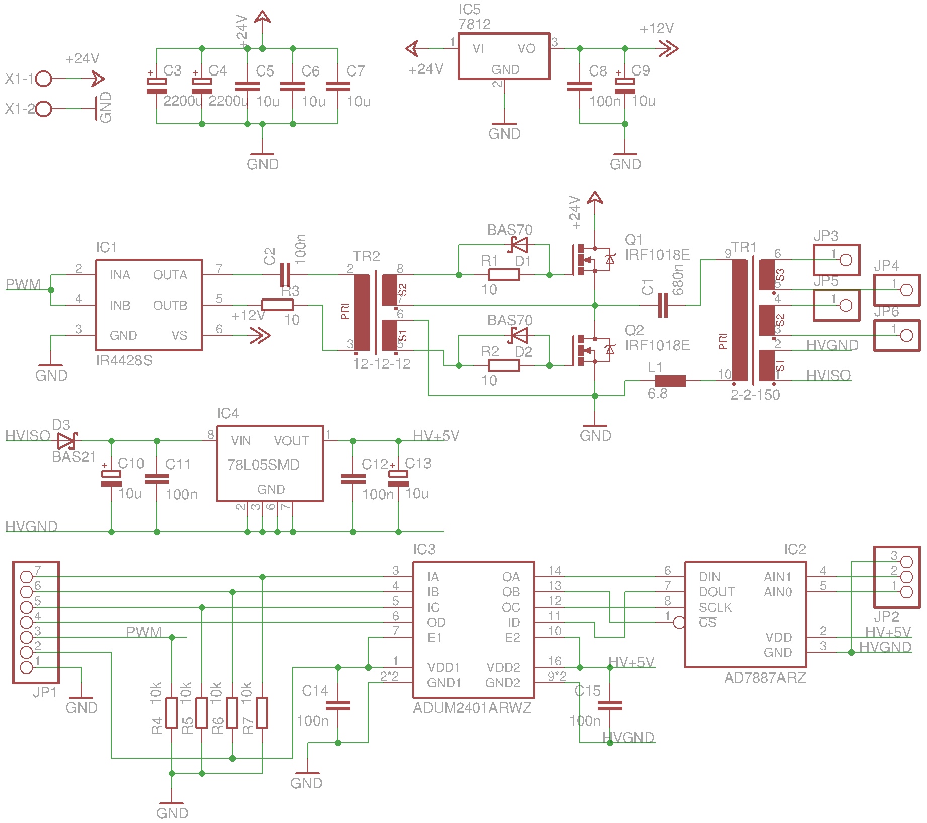
The converter utilizes a half-bridge based on IRF1018E MOSFETs Q1 and Q2, driven using an IRF4428 driver IC2 via a gate drive transformer TR2. The TR2 coils are wound using a 0.03mm² PTFE-coated multistrand wire. The R1 and R2 resistors limit dv/dt. The D1 and D2 diodes increase the speed of gate discharge.
The power transformer TR1 PRI coil is wound using 0.78mm² varnish-covered wire. The TR1 S1 and S2/S3 coils are wound using 0.03mm² PTFE-coated multistrand wire. (In practice, TR1 was wound so that pins 4, 5 and 6 connect to a center-tapped 150-turn coil.) The capacitor C1 and inductor L1 provide the resonant circuit.
The power board provides galvanic isolation using an ADuM2401 digital isolator IC3, which is convenient for isolating a single IC with an SPI interface. The instrumentation is performed with an AD7887 12-bit SAR ADC IC2. The entire isolated section is powered from the power transformer secondary S1 rectified via D3 and stabilized using a 78L05 regulator IC4.
The connector JP1 is the interface for the control board. It provides the isolated SPI interface to the ADC and the frequency input.
The connector JP2 is the low-voltage frontend interface, providing analog inputs. The connectors JP3-JP5 (JP6 is unused) are the high-voltage frontend interface. Using a center tap transformer allows to construct a full-wave rectifier using just two diodes.
Design failures
The design turned out remarkably well. There are a few amends I would do:
-
The BAS70 diode (Vr=70V) initially used breaks down due to transients in S1. It was replaced with BAS21 (Vr=200V).
-
The resonant inductor L1 dissipates unreasonable power, heating up to 110°C with passive air cooling. This can be solved with forced air cooling, bringing its temperature to 75°C, within its working range.
Addiitonally, the TSL1112 inductor series features a plastic case, which needlessly increases thermal resistance. It can be removed using hot air gun.
Replacing L1 with an inductor with same form-factor but smaller value (3.3µH) and thus higher rated current (5.9A), which is substantially higher than average rated input current (2A) did not improve thermal characteristics.
-
The analog input channels should have been RC-filtered on this board. See the layout failures section for details.
-
The low-voltage frontend interface JP2 should have also provided power so that frontend could contain active components.
-
Don’t use tantalum capacitors for the isolated power supply. Replace it with lower ESR ceramics of the same value.
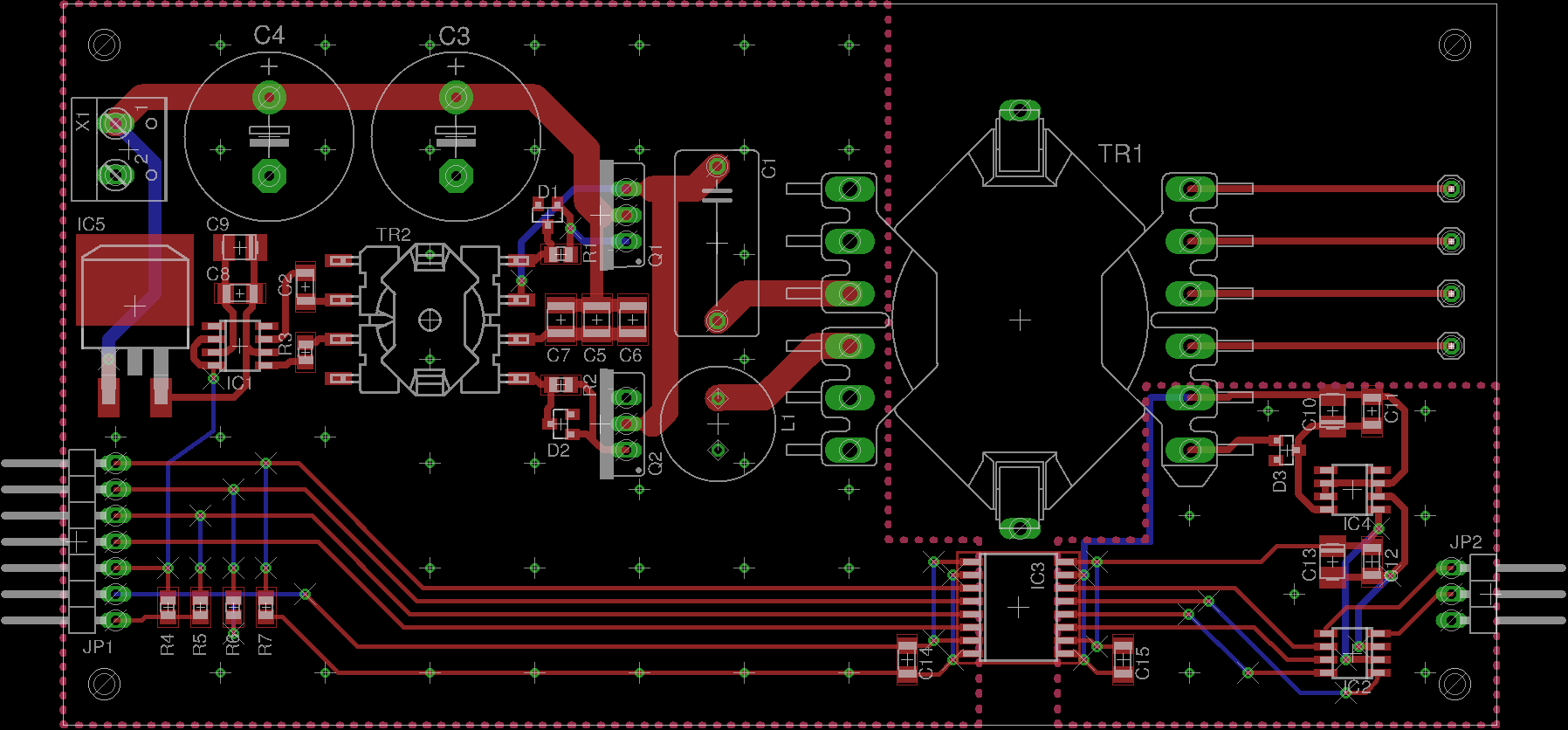
Layout
There are three main layout considerations for this board:
- For the power transformer and FETs, trace inductance must be minimized.
- For the instrumentation ADC, power and analog inputs must be decoupled well to mitigate the noisy environment.
- For the high-voltage traces and wires, enough distance must be maintained to the signal traces and wires.
The layout is as follows:
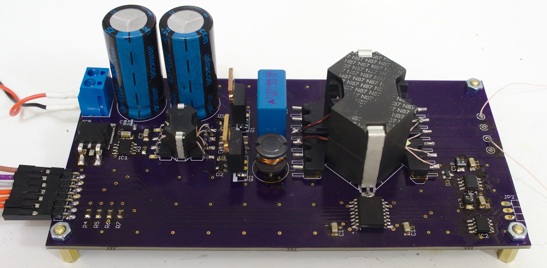
The finished board looks like this:
Layout failures
The transformer driver layout is faultless.
Failures important for the design turned out to be:
-
The TR1 pin 3 is too close to pin 2 (isolated ground) to carry high voltage. It causes arcs to form underneath the coilformer. Skipping the pin 3 fixed the issue.
-
The bypass capacitor C12 for the ADC is too far from it; there is about 1V of ripple in the harshest conditions (arcing).
-
There is no RC filter for the ADC analog inputs near the ADC. Similarly to power bypass capacitor, the RC filter capacitor would have to be immediately adjacent to the ADC.
-
There should be more test points, especially on the noisy isolated side. These test points should feature an adjacent ground point for the oscilloscope ground clip.
Failures whose importance is not clear turned out to be:
-
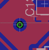
I accidentally left most of the vias that were supposed to connect ground planes isolated from both of them:
Unimportant failures turned out to be:
-
There is not enough space between C3 and Q1 for even a tiny heatsink. However, Q1 and Q2 should have not required a heatsink by design, and indeed they do not.
-
One of the ground vias was too close to a bottom right mounting screw and could probably touch it.
Test and measurement
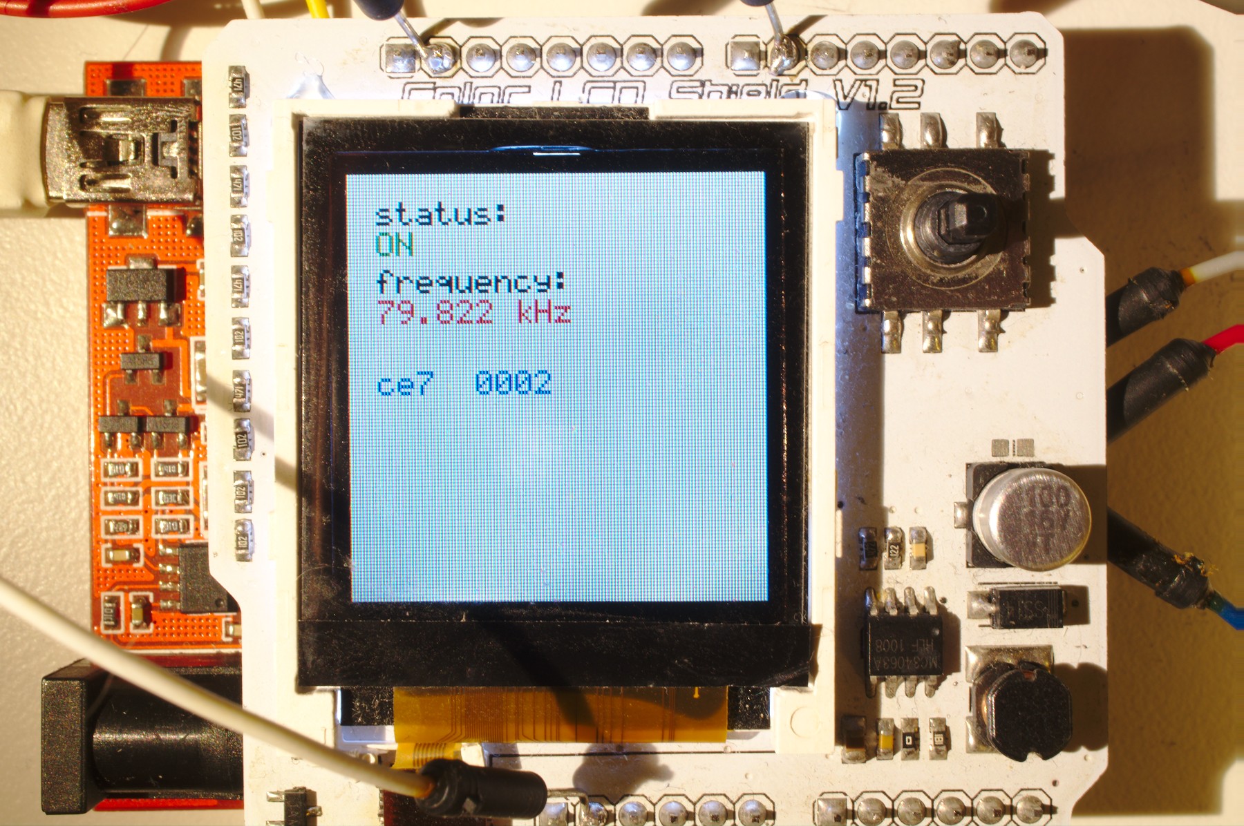
A simple testing rig was assembled using an Iteadmaple and Color LCD shield. The firmware is available on Github.
The firmware currently includes a frequency generator with 1/72MHz pulse width resolution and ADC readout with averaging. The ADC readout is performed in phase lock with the frequency output so as to avoid switching at the same time as ADC sampling.
The Maple to power board connection map is as follows:
| Maple | Power board | Function |
|---|---|---|
| GND | 1 | Supply |
| 3V3 | 2 | Supply |
| D6 | 3 | Frequency |
| D33 | 4 | MISO |
| D32 | 5 | SCK |
| D31 | 6 | NSS |
| D34 | 7 | MOSI |
The firmware offers a simple UI:
The board was stress-tested by continuously powering an arc at 90W for an hour while cooling the board with forced air. There were no malfunctions.
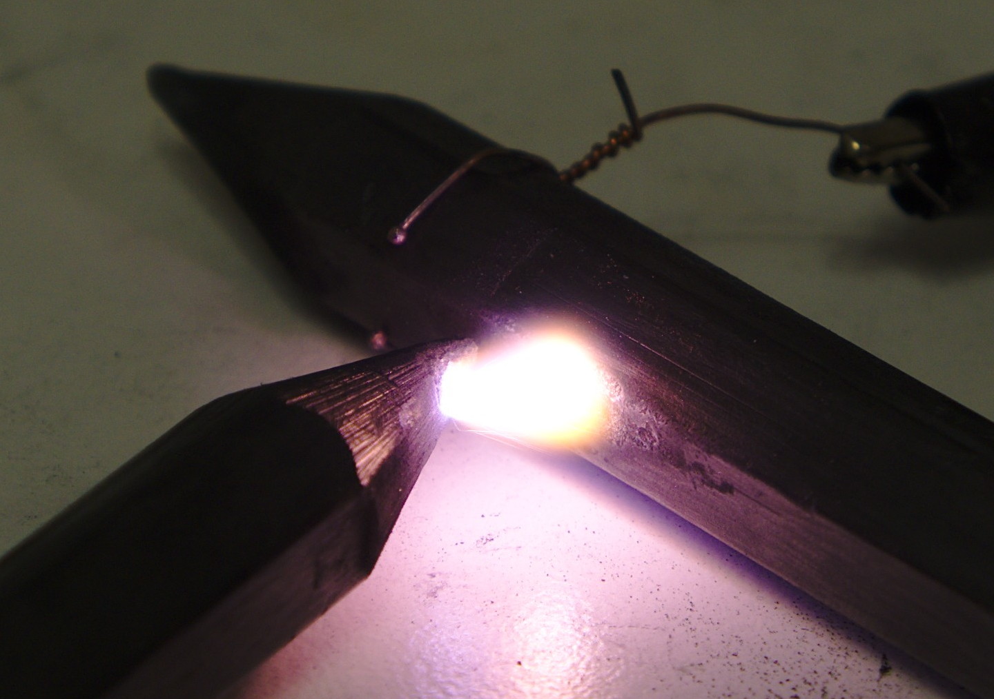
The actual operating environment (a low pressure glow discharge) would be substantially less harsh and noisy; however, this test both provides an upper bound on performance and demonstrates behavior during a failure that arcing would be.
Preliminary specification determined that ADC noise during arcing, after averaging 32 samples, amounts to about 4 bits out of 12. This is not satisfying.
It turns out that using an alligator clip with an oscilloscope probe in a noisy environment leads to acquiring completely worthless data. For instance, I’ve seen 20+V ripple on ADC power rails whereas the real value is under 1V. Using a spring ground clip instead leads to much better results.
Conclusions
A more extensive testing has to be performed to determine performance with a specific frontend; I will start with a simple rectifier frontend. No switching waveforms are provided so far, as the only testing done so far was done with an arc, which is neither a typical nor useful load.
The board will probably have to be respun to obtain better ADC performance.
The power dissipation on the inductor is annoying, but acceptable with forced air cooling.